A Selection Guide to Choose Sputtering Targets for Semiconductors
-
- April 11th, 2026
- 323 views

FREE SEO Topical Map Generator: Find Your Next Content Ideas
The world of semiconductors is intricate and ever-evolving, with sputtering targets playing a vital role in this industry. This article explores sputtering targets, their importance, essential features, and the suitability of semiconductor-grade targets.
What Are Sputtering Targets?
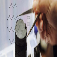
Sputtering targets are critical in the process of physical vapor deposition (PVD), a method used to apply thin films onto various substrates, including silicon wafers in semiconductor applications. These targets are composed of high-purity materials, such as metals and alloys, which, under high-energy ion bombardment, release atoms. These atoms then coat a substrate, forming a uniform thin layer that is crucial for the effective functioning of integrated circuits (ICs).
This thin film layering is indispensable across various applications, such as forming conductive interconnects, creating barrier layers, and developing insulating films in ICs. Sputtering targets come in a variety of compositions and shapes—ranging from pure metals to complex alloys—each selected based on the specific requirements and conditions of the deposition process.
In the semiconductor sector, the quality of sputtering targets directly correlates with the performance and reliability of electronic devices. Thus, selecting the right sputtering target is paramount to ensuring low defect rates and high electrical performance.
Essential Features of Semiconductor-Grade Targets
The essence of semiconductor-grade sputtering targets lies in their material purity, uniformity, customization capabilities, and their role in various deposition environments. Understanding the features can guide manufacturers in selecting the appropriate targets for their needs.
Ultra-High Purity (5N+): Semiconductor-grade targets require extraordinarily high purity levels, typically 99.999% or above. This level of purity is crucial as impurities can lead to higher defect rates, compromising the electrical performance of the semiconductor devices. Such purity ensures the stability and consistency of the films, enhancing device reliability and performance.
Microstructural Uniformity: Uniformity in grain size, density, and crystallographic orientation is crucial for achieving consistent film properties. Microstructural uniformity ensures that the films have predictable and repeatable characteristics, an essential factor when producing devices that demand precision.
Customization: The ability to tailor sputtering targets is a significant advantage. Semiconductor manufacturing processes can vary greatly, necessitating the use of specific shapes, sizes (such as rectangular or circular), and material compositions (including various alloys). This customization allows for the optimization of sputtering targets to suit different process requirements and PVD equipment.
The semiconductor industry utilizes a diverse array of metals and alloys in sputtering targets, such as copper, tantalum, aluminum, titanium, cobalt, and tungsten, each suited for specific layers within a chip. For instance, high-purity copper is often used in conductive layers due to its low resistance, while tantalum serves as a robust barrier layer.
As the semiconductor field progresses towards smaller processes, especially with the increasing demand for high-density and high-performance chips, the reliance on high-quality sputtering targets becomes even more pronounced. Materials like aluminum and titanium are essential for technology nodes requiring stability and anti-interference capabilities, while more advanced nodes leverage materials like tungsten-titanium alloys for specialty applications in memory and gate circuits.