How Physical Vapor Deposition Is Used in Industry: Common Real-World Applications
-

- February 23rd, 2026
- 1,481 views

Get a free topical map and start building content authority today.
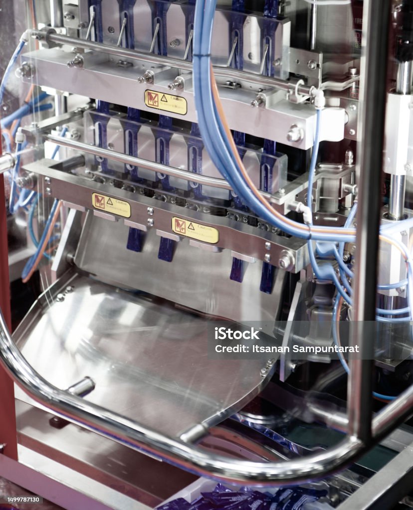
Physical Vapor Deposition (PVD) is a set of vacuum-based coating techniques widely used to deposit thin films and functional layers on substrates across many industries. This article describes common real world applications of PVD, the principal processes (sputtering, evaporation, cathodic arc), and practical considerations for selection and quality control.
- PVD produces thin, adherent coatings for electronics, optics, cutting tools, decorative finishes, and energy devices.
- Typical processes include magnetron sputtering, thermal evaporation, cathodic arc, and ion plating.
- Key benefits: precise thickness control, high purity films, and a wide choice of coating materials (metals, nitrides, oxides).
- Quality and reproducibility are governed by vacuum technology, substrate preparation, and process parameters; standards and laboratory testing support reliable implementation.
Common Real World Applications of Physical Vapor Deposition
Semiconductor and microelectronics
PVD is integral to semiconductor fabrication for depositing conductive and barrier layers (e.g., aluminum, copper seed layers, titanium nitride) on silicon wafers and interconnects. Magnetron sputtering and evaporation provide uniform thin films with nanometer-scale thickness control required for integrated circuits, MEMS, and advanced packaging. PVD is often used alongside chemical vapor deposition (CVD) and atomic layer deposition (ALD) in multi-step process flows.
Optical coatings and display glass
Thin films deposited by PVD create anti-reflective coatings, mirror layers, dielectric stacks, and conductive transparent oxides on lenses, camera sensors, architectural glass, and flat-panel displays. Materials such as silicon dioxide, titanium dioxide, and indium-free transparent conductors are commonly applied by sputtering or evaporation to control optical properties like reflectance and transmittance.
Wear-resistant and tool coatings
Hard coatings such as titanium nitride (TiN), chromium nitride (CrN), and diamond-like carbon (DLC) are applied to cutting tools, molds, and forming dies to increase hardness, reduce friction, and extend service life. PVD coatings are favored for thin, dense layers that maintain sharp tolerances and dimensional stability.
Automotive and aerospace components
PVD is used for components that require corrosion resistance, low friction, or thermal stability: piston rings, valve components, hydraulic parts, and optical sensors. Decorative PVD finishes (e.g., gold, bronze-color coatings) are also applied to trim and interior hardware for durability and aesthetics without plating baths.
Medical devices and implants
Biocompatible PVD coatings, including certain nitrides and oxides, can improve wear resistance and reduce ion release on surgical instruments, orthopedic implants, and dental tools. Process control and surface characterization are critical to meet medical device regulations and biocompatibility testing requirements.
Energy and photovoltaics
PVD contributes to solar cell manufacturing for transparent conductive layers, metal contacts, and reflective back coatings. Thin-film batteries and solid-state device research also use PVD for electrode and electrolyte layers in laboratory and pilot production.
How PVD Works: Key Processes and Materials
Magnetron sputtering
Magnetron sputtering ejects atoms from a solid target using a plasma; atoms then condense on the substrate as a film. It offers good step coverage, compositional control for alloys and compounds, and is commonly used for metal, oxide, and nitride films.
Thermal and electron-beam evaporation
Evaporation heats source material so that vapor reaches the substrate. It enables high deposition rates and is useful for metals and some oxides, but may have lower film density than sputtering unless assisted by ionization.
Cathodic arc and ion plating
Cathodic arc produces highly ionized metal vapor suitable for hard coatings; ion plating combines vapor deposition with ion bombardment to enhance adhesion and film density. These are often used for wear and decorative coatings.
Benefits and Limitations
Benefits
- High film purity and controlled stoichiometry for compound coatings.
- Thin, uniform layers with precise thickness control (nanometer to micrometer scale).
- Compatibility with many substrate materials (metals, glass, silicon, some polymers with temperature limits).
- Environmentally cleaner than some wet plating processes because PVD uses no plating baths.
Limitations
- Vacuum equipment and process control add capital and operational cost.
- Line-of-sight nature of PVD can limit coating of deep recesses without shadowing; advanced tooling and rotation often mitigate this.
- Temperature-sensitive substrates may restrict some PVD methods unless low-temperature processes are used.
Quality, Standards, and Industry Guidance
Process control and testing
Reliable application of PVD requires monitoring vacuum level, deposition rate, substrate temperature, and plasma parameters. Post-deposition characterization uses profilometry, ellipsometry, X-ray diffraction (XRD), and adhesion testing to verify film thickness, composition, crystallinity, and durability.
Standards and organizations
Guidance for vacuum and thin-film metrology is available from standards organizations and technical societies; laboratories often reference international standards for coating thickness and adhesion. For technical reference and measurement best practices, consult resources from the National Institute of Standards and Technology (NIST) and professional societies such as the Society of Vacuum Coaters (SVC).
For more on measurement science and thin-film metrology, see the NIST website: NIST.
Selecting a PVD Process for an Application
Match performance to functional need
Selection depends on required film material (metal, nitride, oxide), thickness, adhesion, surface finish, part geometry, and production volume. High-volume electronics often favor sputtering for uniformity, while tool shops may choose cathodic arc or ion-plating for hard coatings.
Evaluate cost and scalability
Evaluate capital cost, throughput, yield, and maintenance. Pilot runs and standardized tests help anticipate production challenges such as target poisoning, subtrate fixturing, or contamination control.
Environmental and safety considerations
PVD avoids liquid chemical waste from plating baths, but vacuum pumps, target materials, and process gases require proper ventilation, handling, and recycling practices in accord with local workplace safety regulations.
Frequently Asked Questions
What is Physical Vapor Deposition used for?
Physical Vapor Deposition is used to deposit thin films for electronics, optics, wear-resistant tool coatings, decorative finishes, medical device surfaces, and photovoltaic layers. It supports applications that need precise, uniform, and adherent coatings across diverse substrates.
How does PVD differ from Chemical Vapor Deposition (CVD)?
PVD is a physical process that transports vaporized atoms in a vacuum to form a film, while CVD relies on chemical precursors that react on the substrate surface. PVD generally gives high-purity films with simpler byproducts, whereas CVD can deposit conformal coatings on complex geometries.
Can PVD coat plastics or temperature-sensitive parts?
Yes, but process selection is critical. Low-temperature sputtering or using cooled fixtures and short deposition cycles can make PVD compatible with some polymers; however, thermal budget and adhesion-promoting pretreatments must be evaluated.
How is coating performance verified?
Performance is verified by measuring thickness (profilometry, ellipsometry), composition (XPS, EDS), hardness and adhesion (scratch and nanoindentation tests), and functional tests such as corrosion resistance or optical transmission depending on application requirements.
Are there environmental advantages to PVD?
PVD generally reduces hazardous liquid wastes compared with plating processes. Energy use and vacuum pump emissions should be managed, and material recycling programs for targets and sputter byproducts can reduce environmental footprint.